You’ll need a bit of multilayer PCB experience (4-layer PCB to be exact). But don’t worry, this PCB is simple and not that advanced. If you’ve routed 2-layer PCBs before, this shouldn’t be an issue.
MAke your Board Outline
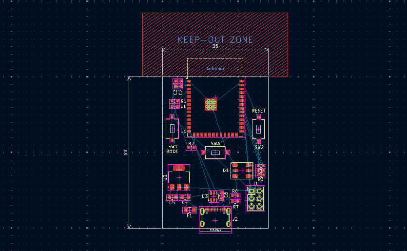
Try to estimate your board outline enough to contain all of your components. Remember the rule to keep the PCB antenna part cleared below. Here, an approximate value of 35mm x 50mm board area is made, although this can still change.
PLacing the Components
For the placement, it’s necessary to have clearance for the PCB antenna of the ESP32-S3 WROOM. With this, place the keep-out zone area outside of the board edge.
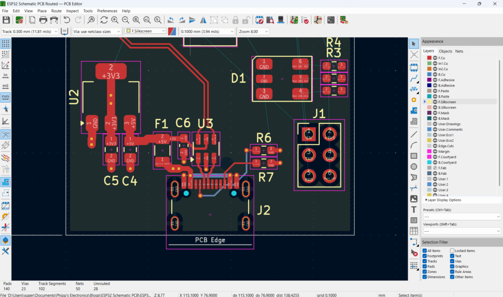
The USB-C is placed on the board edge for comfortable access of the user. The ESD diodes are placed near it too. Remember to keep bypass capacitors near the power lines for adequate filtering. Also, follow the precedence of filtering with a large cap first, and then a smaller cap next. More importantly, allow space for the USB traces to reach the USB port of the ESP32. Below is a rough layout.
Assigning Nets to Copper Fills on Selected LAyers
As this is a 4-layer board with a USB trace, it’s important to assign proper nets to the copper fills of the relevant layers. With this, layer 2 is ground while layer 3 is +3.3V.
Begin Routing your Board
Route the USB Traces First
As the USB traces are controlled impedance lines, it’s important to make room for them first. You can adjust the traces or move components along the way. Below is just a rough example.
IMPORTANT: Please note that the two D+ pads of the USB-C port should be shorted or routed together, as well as the two D- pads. This is not shown in the project. USB-C is a reversible connector. One pair should line up correctly with the host/device, regardless of how you plug it in.
Route the Power Lines Thicker
As these traces carry more current, thicken them according to their current specifications (usually 0.5mm – 1mm, or even more). You can make some track specifications/rules on Board Setup. It’s recommended to use multiple vias near power pads (2 vias). Use 0.3–0.4 mm drill diameter with 0.6–0.8 mm pad size for power vias.
Example Layout of Power and USB
Below is an example routing layout for the USB-C, ESD diode, and Power components.
IMPORTANT: Please note that the two D+ pads of the USB-C port should be shorted or routed together, as well as the two D- pads. This is not shown correctly in the project. USB-C is a reversible connector. One pair should line up correctly with the host/device, regardless of how you plug it in.
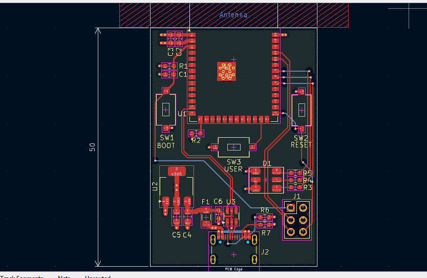
Continue routing the other components. Utilize the top and bottom layers for your signal routes. Use the X-Y rule to minimize tangled routings. Remember, since there is a ground plane on layer 2, signal interference between the top and bottom layers is non-existent.
Below is an example route of all the components. Note that this is not the final layout yet.
Your PCB design does not end with routing all your components. Remember, you have an RF design. To keep the integrity of your RF signals, ensure tight grounding through via-stitching (1mm – 2mm apart) near the board edge antenna side. Additionally, add a ground copper fill.
Next, drop ground vias all over your board. This will guard your design against ground bouncing. Don’t forget to add the copper pours.
Finalize your Board
You’re nearly finished with your design. Finalize the silkscreen layer and add or modify necessary reference designators and texts.
If all is well, you should be able to generate a 3D model of your ESP32 PCB design.
IMPORTANT: Please note that the two D+ pads of the USB-C port should be shorted or routed together, as well as the two D- pads. This is not shown in the project. USB-C is a reversible connector. One pair should line up correctly with the host/device, regardless of how you plug it in.