Do you want to know how to generate Gerber files in KiCAD? Do you want these outputs sent to your PCB Manufacturer? See the article below to find out.
Introduction
Generating fabrication outputs from your PCB design is a major requirement for PCB fabricators to be able to manufature your boards. These outputs usually contain your Gerber and drill files. This article will help you generate these files easily from your KiCAD PCB design suite.
Generate your Gerber Files in KiCAD
After finishing your PCB design (as in the previous blog about KiCAD’s PCB Editor), it’s already possible to manufacture your board. With this, Gerber files should be generated. These files comprise routing and detail layers such as top and bottom copper, silkscreen, solder paste, solder mask, and edge cuts.
To generate Gerber files in KiCAD, go to the PCB Editor and choose File -> Fabrication Outputs -> Gerber.
Here, check the layers you want to come along with your fabrication outputs on the left side. Usually, you don’t have to change the default checked settings. After this, you can check several options your manufacturer requires for your Gerber output. Here (as is the case for JLCPCB as the manufacturer), the checked items are:
Plot reference designators
Check zone fills before plotting
Use Protel filename extensions
Subtract soldermask from silkscreen
Use extended X2 format (is don't care)
Before generating your Gerbers, make sure you define an output directory above.
Generate your Drill Files in KiCAD
Generating drill files is important especially if you have drill holes, through hole components, and vias on your board. To do this, still, on the Plot window, click Generate Drill Files… below.
Check the settings your PCB manufacturer requires. Below are the requirements for JLCPCB for example:
Use alternate drill mode in Oval Holes Drill Mode
Absolute in Drill Origin
Millimeters in Drill Units.
Millimeters in Drill Units
Decimal format in Zeros Format
Click Generate Drill Files and then Generate Map File.
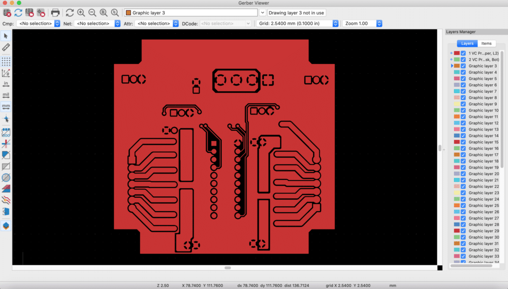
Check your Outputs with Gerber Viewer
You don’t need a third-party Gerber viewer to check on your fabrication outputs. You’ll already see a Gerber Viewer on the KiCAD main screen. Click on this and then select and load your Gerber files for viewing.
You're Ready to Go!
Pack all these output files into one zip file to ready them to send to your PCB manufacturer. The next blog will lead you to generate your assembly files.