Do you want a free and open source software to do your PCB designs? Want a complete software package such as KiCAD to be able to design and fabricate your boards? Read through the article to find out.
Introduction
You may have wanted to create sophisticated PCB designs but can’t afford an expensive PCB design software. You’ve searched for some free PCB design tools but are not satisfied with their capabilities and functions. So you wonder, is there such a PCB software suite that can do schematic capture, PCB layout, and 3D rendering all in one package with a free price tag? Worry no more; KiCAD has all of these features.
KiCAD is entirely free and open source. Volunteering engineers created it to help the open source community thrive in hardware design. It’s a complete PCB suite running it’s workflow in an IDE (Integrated Development Environment). It’s more than you’d hope for if your on a hardware design budget.
What are the capabilities of KiCAD
KiCAD has almost everything. It has schematic capture, parts library management, PCB layout tools, fabrication outputs, and even 3D rendering of your boards. If you want to start your PCB designs with the end goal of manufacturing it, KiCAD is the way to go.
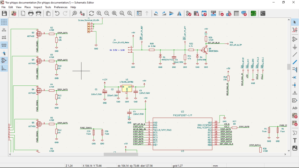
Schematic Editor
KiCAD has schematic generation and editing capabilities. It has a neat user interface and editing area. You can easily add a part symbol, connect the symbols, add net names, and add hierarchal sheets from the toolbar on the right. You can even add bitmap images to your design. Additionally, DRC, BOM, and netlist generation can all be done in a breeze in this editor. See the tutorial for schematic entry in KiCAD.
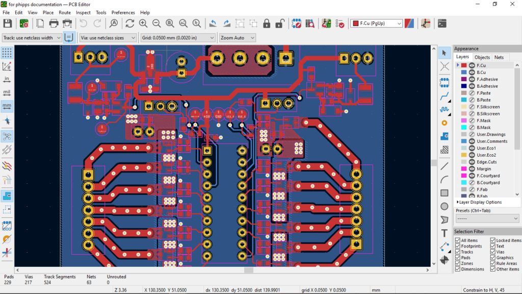
PCB Layout
KiCAD has an excellent PCB layout editor. Navigating your board in KiCAD is a breeze; you can use your mouse’s scroll key to zoom in to your design while right-clicking to pan your view. Routing is intuitive as it always suggests a best route strategy as you connect your pins.
Additionally, all layer elements are included in you board, such as silkscreen, solder mask, paste, edge cuts, courtyard, and many user-defined layers. In KiCAD, you can create copper zones to your liking by defining a filled zone drawn freely with your mouse. There are also specific steps to incorporate DXF drawings on your board.
You can easily create manufacturing plots and assembly data that you can send to your PCB fabricator once you finish your PCB design.
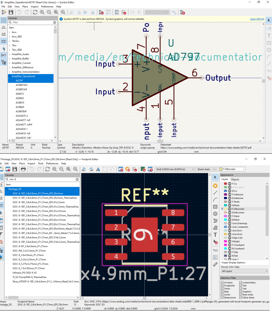
The Symbol and Footprint Editor contains hundreds of schematic symbols and PCB footprints in industry standard forms and packages. The library contains most well-known electronic parts, and it keeps growing. Additionally, you can download schematic symbols and footprints in KiCAD format from different electronics components vendor sites. You can also edit or create your own footprint using components from the parts library as base.
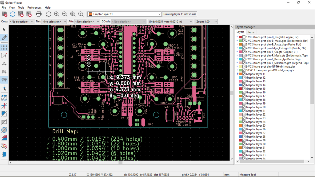
Gerber Viewer
KiCAD’s Gerber viewer is a welcome addition to KiCAD’s set of PCB design tools. With this, you don’t need an external or third-party Gerber viewer.; you can access Gerber viewer in KiCAD’s very own IDE.
You can accurately measure points on your design using real-time coordinate tracking. Different layers of your board can be added and stacked up in Geber viewer anytime.
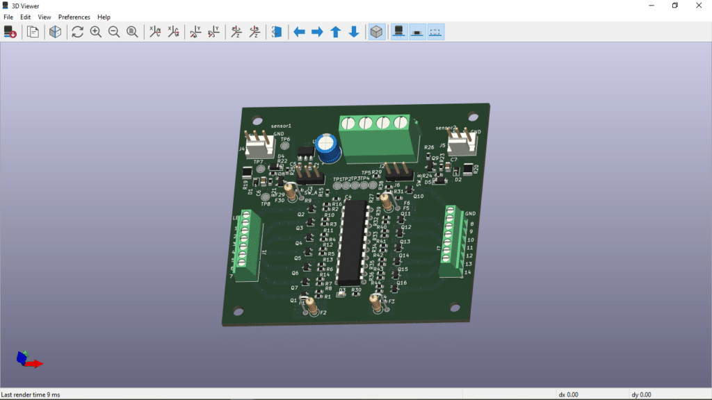
One of the more interesting capabilities of KiCAD is generating a 3D model of your board. This capability is seldom heard of in free PCB design software. With this, you’ll get a better glimpse of your overall PCB design and assembly. 3D viewing may be a necessity especially if you have complex assembly requiring components with different heights as well as complicated packages.
Conclusion
If you’re looking for a complete, easy to work with PCB design software that’s totally free, go with KiCAD. With KiCAD, you can design your PCB’s and generate manufacturing outputs easily all in one IDE.