Would you like to know how to communicate with a PCB fabricator to get your PCBs manufactured and assembled? Get the details here including how to ship the boards
Introduction
Getting your boards manufactured by a PCB fabricator is no trivial task. First, you have to prepare your Gerber outputs correctly. Next, if you need your fabricator to assemble your boards, you must also generate your BOM and position files. After that, the next thing to do is send these files to your fabricator. Add to these other settings and specifications needed to manufacture your boards correctly.
Choose a Reliable and Trustworthy PCB Fabricator
Choosing a trustworthy PCB fabricator is essential to getting your boards manufactured according to your specifications. There are several well-known fabricators that you can go to. To name a few, there is JLCPCB, PCB Cart, PCB Way, and others. These Chinese-based companies will happily receive your fabrication data, receive your payments, then ship your finished boards to you in less than a month. Local manufacturing is also gaining ground again, and you should be able to see different kinds of them in your country.
An Example Transaction with a Known PCB Fabrication Company.
Here, we’ll make a simple transaction with JLCPCB. We’ll use the fabrication outputs of the example board we’ve made from past blogs of this series. By the way, ensure you’ve put your Gerber files into one zip file.
First, go to the JLCPCB homepage, then make your account. Sign in if you have to.
Next, click Instant Quote and then add a Gerber File. Upload the zip file you made earlier. You should see it successfully uploaded.
Now try to use the Gerber Viewer tool of JLCPCB to review your board.
Your next step is to review different PCB parameters such as layers, PCB color, PCB thickness, silkscreen color, and the like. You can also check the special inspection services that JLCPCB can offer.
As we want to assemble our boards, turn on the PCB Assembly switch to bring out more options. Check the options you want and then confirm.
The next part reviews your PCB and inserts your BOM and CPL (position file). Find the files mentioned in your project directory or where you’ve generated them (as discussed in the previous blogs). After this, a graphical representation of your board with components will be shown to get an overview of what it looks like. Note that the placement of the actual components may need verification from your order history.
After placing your order in your cart, you can proceed with payment and delivery options.
Continuos communication
Communication with your fabricator does not end here. They may ask questions regarding your design, placement, etc. Always check your email regarding this.
Wait and Receive your PCB
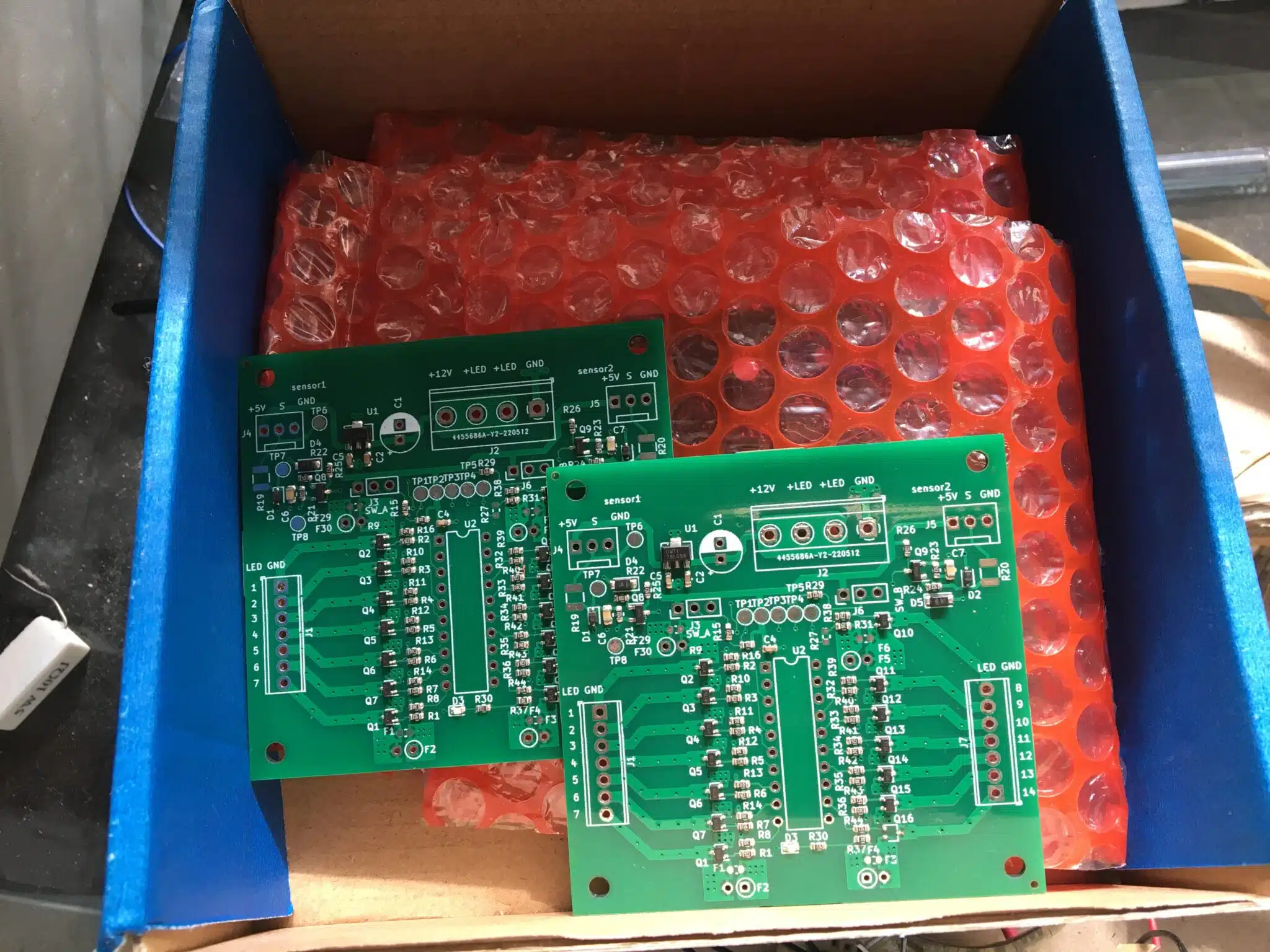
If all goes well, you should receive a parcel with your assembled PCB inside. Enjoy! This is the end of the PCB Design Tutorial Series in KiCAD. 🙂