Would you like to have a PCB design tutorial in KiCAD? Know how to route your PCB’s and design them using KiCAD’s PCB layout editor by reading through this article.
Introduction
KiCAD has a complete PCB design suite, including a PCB layout editor. The editor’s primary purpose is for you to be able to interconnect all of your parts footprint via copper tracks. You can do this by routing those tracks on single or multiple layers on a PCB, optionally connecting them through vias.
KiCAD PCB Editor has complete tools and functionalities to accomplish the task mentioned above, and they include:
An intuitive PCB routing tool
Multiple Layer tools
Adding copper zones or filled zones
Adding Keepout area rules
Wire length tuning
Adding design rules and constraints
Fabrication outputs
and others
This tutorial will focus on using basic PCB design and layout tools in KiCAD.
How to Start Making your PCBs
Last time, a fully annotated schematic was made from the schematic entry in KiCAD blog. Each part was also given a footprint. With this, you can already make physical parts that can be placed on your printed circuit board. To start, in KiCAD schematic, click the Open PCB in Board Editor button above.
After this, the PCB Editor should show up. Next, click the Update PCB with changes made to schematic icon. The Update PCB with schematic window should appear along with the changes. If everything goes well, click Update PCB.
Now place the parts that were generated on the current schematic sheet.
View the process in the video demonstration below.
Begin Making a Board Outline
Begin making a board outline by clicking the Edge Cuts layer on the right and then clicking the Draw a Rectangle button. Choose an appropriate linewidth for this such as 0.5mm.
Make your Components Placement
You can start placing the components according to your design’s specifications. Drag and drop these parts anywhere on your board. Press the R key to rotate the parts. You can turn on and off detail layers (such as silk, fab, and others) as you do your placement. You can still adjust your board outline to meet your board’s placement strategy.
Create a Ground Layer for your Board
Creating a ground layer on your board is an excellent way for your components to connect to a common ground plane. This eliminates “ground bounce” issues and creates a low-impedance reference point.
First, select the bottom layer by clicking B.Cu on the Layers tab on the right under Appearance. After that, click the Add a Filled Zone button on the right toolbar. Create your ground copper pour on this layer and select the GND net.
Begin Routing your Board
You can begin routing your board. First, select the F.Cu layer as your routing layer. Next, click the Route tracks button on the right toolbar. You can then begin routing tracks to and fro your component pads to connect them with one other.
Press E to change track thickness (as when creating power tracks), then input the track width.
Press V to create a via as you route your tracks. You can also create a via by clicking the Add free-standing vias button on the right toolbar.
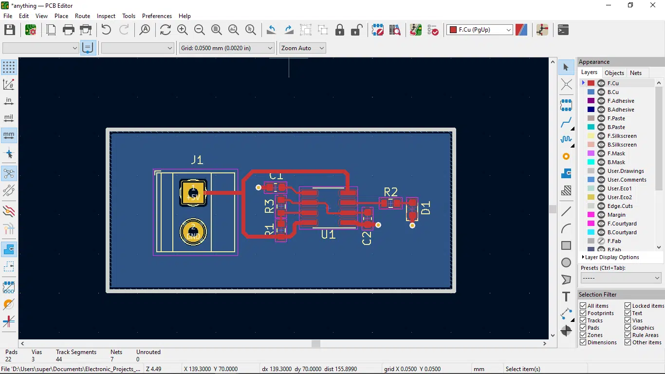
Your Board's Final Look
After all is done you’ve just created your printed circuit board in KiCAD. What’s good about this software is that you can instantly generate a 3D view of your board. To do this, simply press the Alt-3 keyboard shortcut.
All is well that you’ve made your PCB design in KiCAD using this tutorial. Your next step should be to create fabrication outputs to manufacture your boards.