Want to make your own custom ciruit using an ATMEGA328P chip? Not wanting an Arduino UNO with it? Read along to know how to do some ATMEGA328P standalone programming.
Introduction
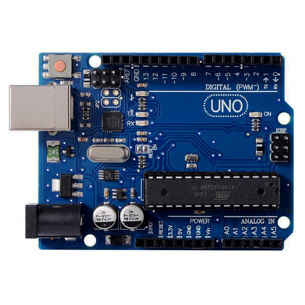
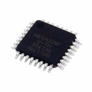
The ATMEGA328P chip series is one of the most popular chip for the Arduino enthusiast. You’ll see this device as the staple chip in the Arduino UNO. Interestingly, the UNO is cleverly constructed so you can place and connect it anywhere inside your projects along with other components or devices. However, what if you wanted a custom board or circuit created for your ATMEGA328P chip? How are you going to program it? This article details how you can do ATMEGA328P standalone programming.
Understanding The Programming Modes
First of all, you have to understand the different programming modes available for your ATMEGA328P chip. These modes are In-System Programming mode (ISP) or programming serially in Bootloader mode.
Programming in In-System Programming Mode (ISP)
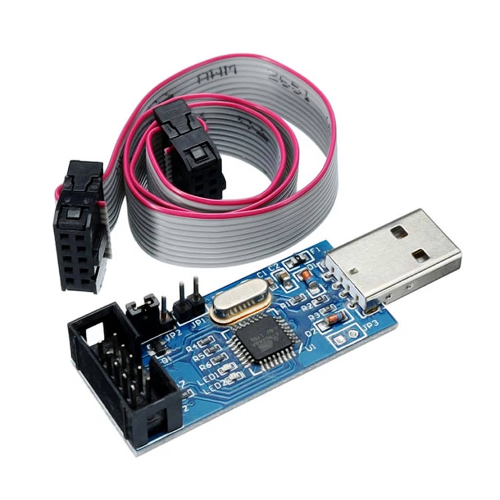
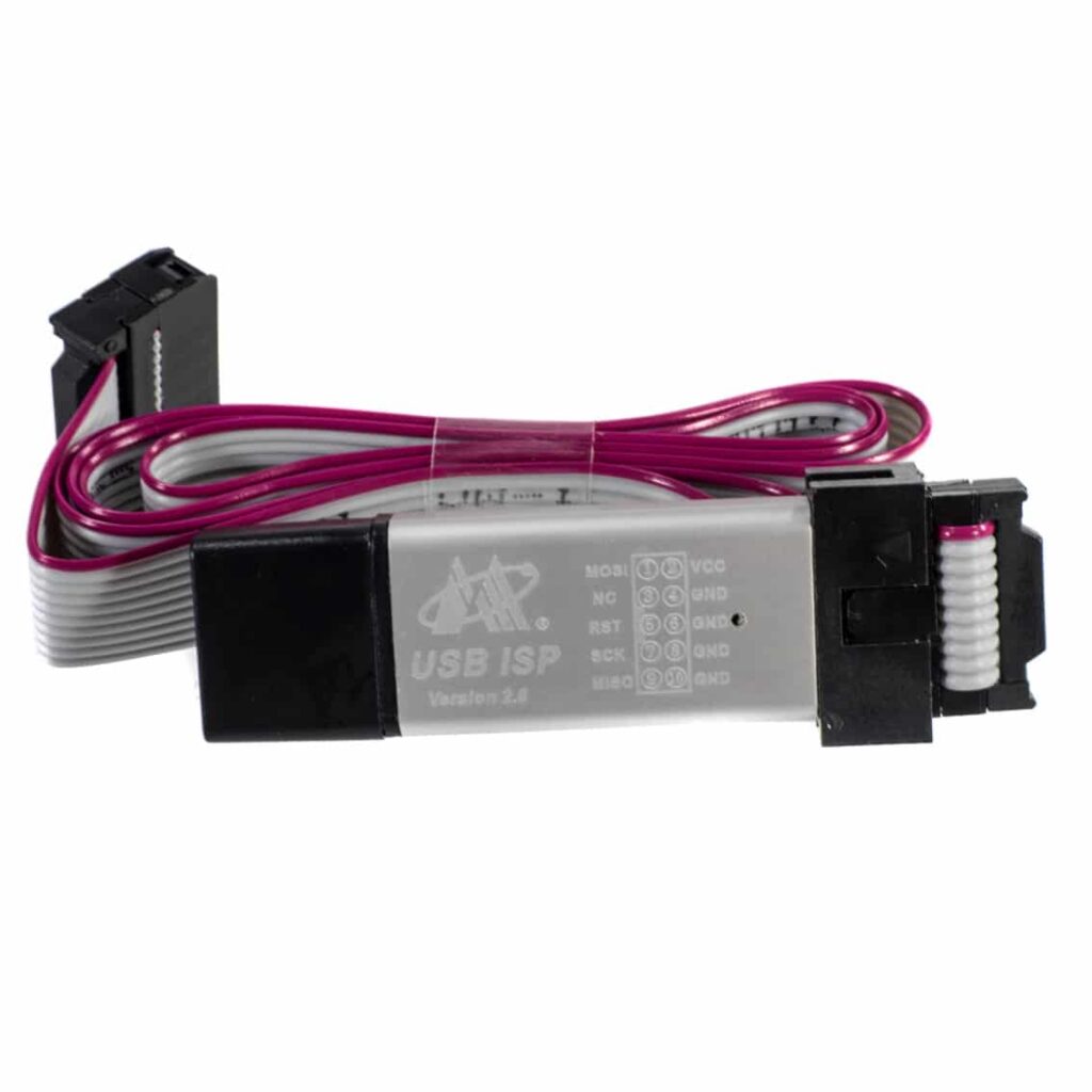
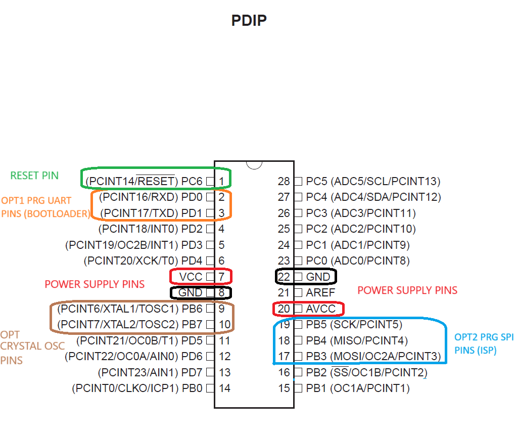
Programming in ISP is the direct means of programming the ATMEGA328P. In this mode, you can program almost anything on the chip. You can program the FUSES (clock source, Brownout detection, Reset pin function, etc.), the EEPROM, and the entire flash area. Besides, programming in ISP is more secure and faster. You can also program bootloader code using only ISP. However, ISP requires an ISP programmer (usually with a 6 or 10-pin ATMEL ISP header). The ISP pins on the ATMEGA328P are the SCK, MISO, MOSI, and RESETpins.
Programming in Bootlader Mode
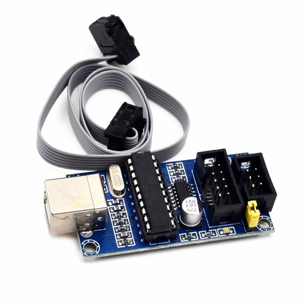
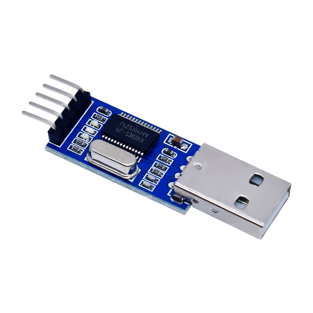
If you don’t have an ISP programmer and all you have is a simple serial interface hardware (such as a USB-to-UART module), you’re better off programming in Bootloader mode. However, note that you should have programmed the bootloader code in ISP mode first already. It is more convenient to program in bootloader mode especially in the field as an available serial interface module can be used. The UART pins available in bootloader mode for the ATMEGA328P chip are the RXD and TXD pins.
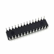
Understanding the Pin Layout of the ATMEGA328P
If you’ll open an old ATMEGA328P datasheet (by the way, Microchip has already EOL’d the PDIP version), you’ll see the device pinout.
The pinout above is labeled for convenience for use in stand-alone programming. Later, a simple practical circuit can be constructed with this.
About Connecting the Power Supply Pins
To successfully program the device, you’ll need to first connect the power supply pins VCC, GND, and AVCC pins. The AVCC pin should be connected to VCC (or with a filter) for proper device operation, or else, the device might not operate. This AVCC pin is utilized in the analog peripherals of the microcontroller.
About ConNecting the Reset pin
If you’re programming your ATMEGA chip with default FUSE setting values and using the UART pins in bootloader mode, it’s advised to pull the RESETpin to VCC using a 10K ohm resistor. This should bring the device out of reset when in need during programming. Alternatively, this RESET pin can be repurposed to be a GPIO pin although this is beyond the scope of this topic for now.
About Connecting an External Crystal Oscillator
It’s recommended to place an external crystal oscillator together with matching NPO ceramic capacitors to pins 9 and 10 especially if you’re programming your ATMEGA chip with default fuse settings and you’re in UART Bootloader mode. The reason is the default fuse setting uses an external crystal oscillator. Note that the oscillator setting can be burned in the FUSE bit settings. It’s possible to use the internal oscillator too. In case you want to change FUSE bit settings you’ll need an ISP (In-System programmer).
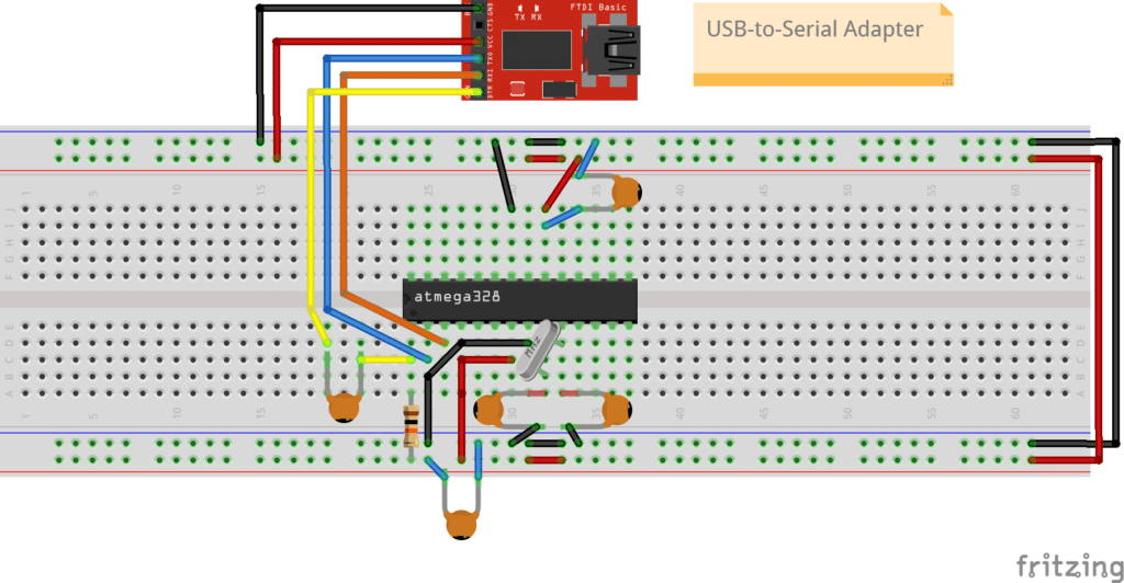
Programing Using a USB-to-Serial Port Adapter (Bootloader Mode)
Here are the basic connections if you’re programming in bootloader mode using the UART pins of the ATMEGA328P.
USB-to-Serial Adapter
ATmega328P
VCC (5V)
VCC (Pin 7)
GND
GND (Pin 8)
AVCC (pin 20)
GND (pin 22)
TXD
RXD (Pin 2)
RXD
TXD (Pin 3)
DTR
RESET (Pin 1) via a 0.1µF capacitor and RESET (Pin 1) pulled up to Vcc via 10k resistor.
OSC1 (Pin 9) via XTAL and NPO Cap to GND
OSC2 (Pin 10) via XTAL and NPO Cap to GND
Notice that the DTR pin is connected in series to a 0.1uF capacitor to the reset pin. This is for automatic rest of the chip after programming.
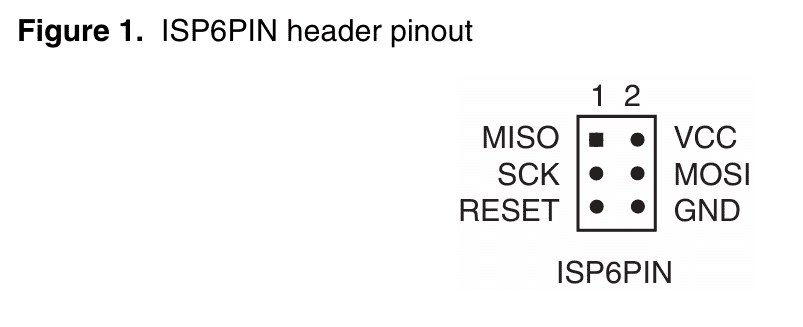
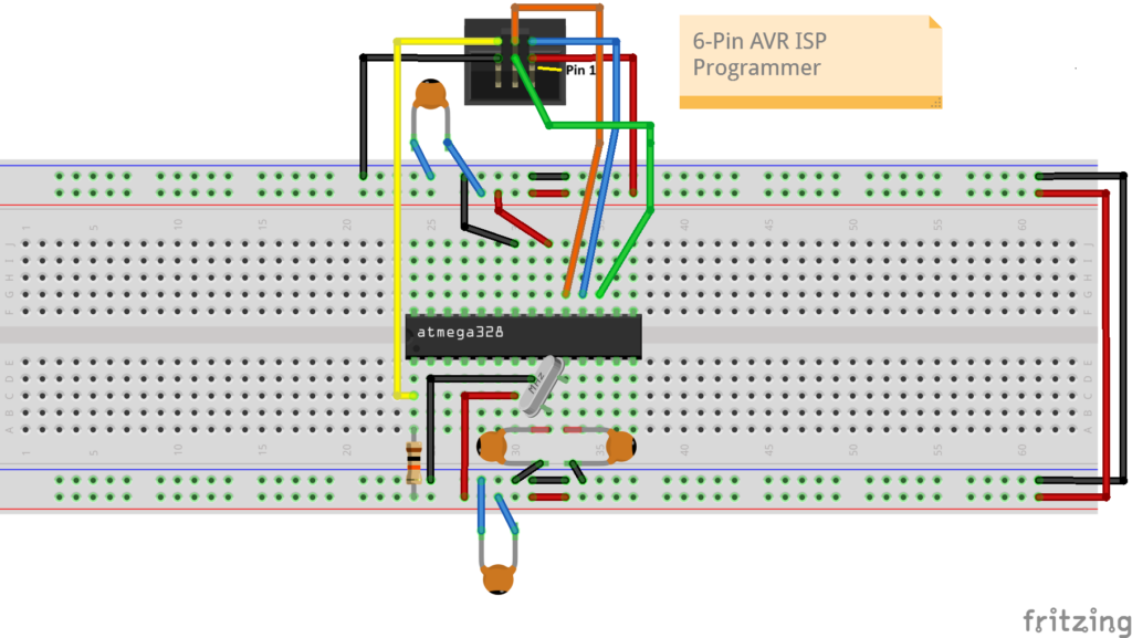
Programming Using an External ISP Programmer
Here are the basic connections if you’re programming in ISP mode using the SPI pins of the ATMEGA328P.
6-pin ISP Programmer
ATmega328P
VCC
VCC (Pin 7)
GND
GND (Pin 8)
MOSI
MOSI (Pin 17)
MISO
MISO (Pin 18)
SCK
SCK (Pin 19)
RESET
RESET (Pin 1) - pull up to VCC via 10K resistor
AVCC (Pin 20)
GND (Pin 22)
OSC1 (Pin 9) via XTAL and NPO Cap to GND
OSC2 (Pin 10) via XTAL and NPO Cap to GND
You’ve just learned the various modes and connections to do ATMEGA328P standalone programming. The next part will teach you how to upload firmware for the different programming modes using Arduino IDE.