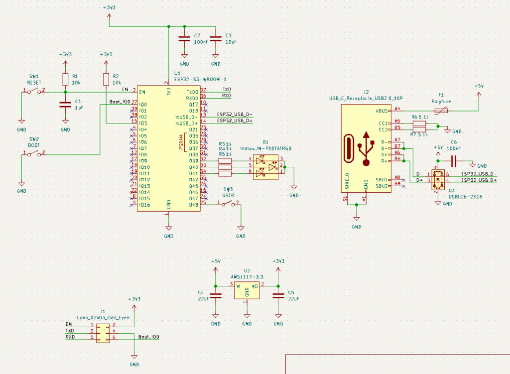
Below, you’ll find a basic schematic of an ESP32-S3 circuit, featuring a USB-C for port and power together with a UART port. Both USB and UART ports can be used for programming. Additionally, there are reset, boot, and a user button. An ESD diode IC is coupled with the USB-C to protect the ESP32 from electrostatic discharge. A 1A polyfuse is also added as safety so that the circuit can cut off current if it reaches above 1A. For signalling, an RGB LED is added.
Note here that this is just a basic ESP32 schematic. The other ports are left unconnected, and it is up to the user to route these ports for other purposes (such as connection to I/O headers).
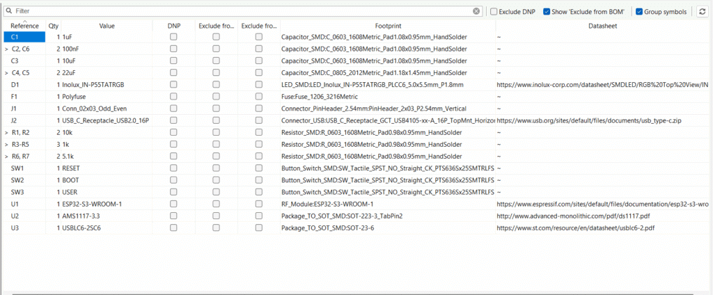
As this schematic was generated in KiCAD, you can refer to the BOM list below. This list includes the symbols and the footprint values used accordingly.
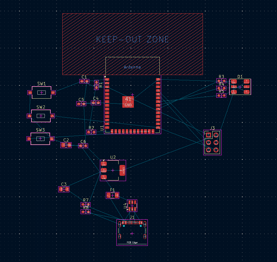
Now that you have a complete schematic, you can generate your PCB. Below is an example of loosely placed components not yet on a board.
Board Stackup Setup
Before actually placing and routing the components, you should set up your board. Note that an ESP32-S3 circuit works well with a 4-layer board because:
The wireless part works well with a solid ground plane, preventing RF reflections and improving the radiation pattern and gain.
High-speed impedance lines, such as USB, require impedance-matching traces that rely on a solid ground plane on L2.
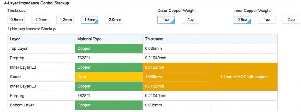
Below are the 4 Layer stackup setting values taken from JLCPCB (PCB Manufacturer) with the common 7628*1 Prepreg. You need these values to route a USB 2.0 differential line successfully.
Additionally, below is an impedance calculator you can use as reference for your 90 ohms USB 2.0 differential pair trace.
If you’re wondering why there are specific thicknesses on some layers, it’s because of the requirement of USB 2.0 Differential Impedance Controlled lines that will be discussed next.
Below is an example of a 1.6 mm-thick 4 Layer board stackup setting in KiCAD. Note that these settings are populated with default values first. You must change them according to your PCB manufacturer’s capabilities.
Creating a Net Class for the USB Differential Lines
To be able to route USB traces easily, it’s recommended to use the Net Class function of KiCAD. Open KiCAD schematic and assign a Net Class to the nets /D+, /D-, /ESP32_D+, and /ESP32_D-
Next, open KiCAD PCB and assign the Net Class Differential Trace Width and Space of the pair of nets assigned. Below is a sample routing sequence.
IMPORTANT: Please note that the two D+ pads of the USB-C port should be shorted or routed together, as well as the two D- pads. This is not shown in the project. USB-C is a reversible connector. One pair should line up correctly with the host/device, regardless of how you plug it in.
Now that you’ve prepared your PCB and board stackup settings, you can continue to make a board outline and route your actual PCB.